TSMC advances A14 lithography with AI in 2nm race as Intel responds
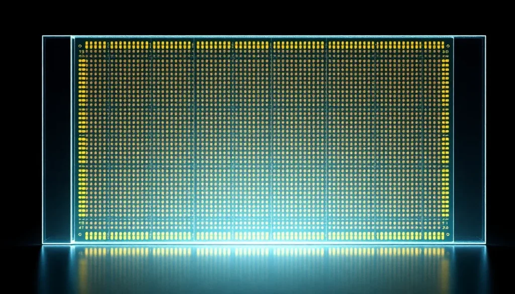
The semiconductor landscape is undergoing a radical transformation, where innovation is driven not only by physical advancement in nodes but also by how chips are designed and manufactured. In this high-stakes environment, TSMC, the Taiwanese semiconductor giant, is at the forefront, demonstrating how artificial intelligence (AI) is revolutionizing the development of its advanced nodes, specifically the A14 at 1.4 nm. Meanwhile, Intel is reacting by bolstering its lithography capabilities with additional state-of-the-art High-NA EUV scanners from ASML. The question looms: who will emerge victorious in this race for technological supremacy?
Although it may seem counterintuitive, the upcoming nodes are already considered outdated before their debut. The real competition lies in the future, with both companies preparing to face off in 2027 with Intel’s 14A and TSMC’s A14. This article delves into how both giants are approaching this battle of innovation, focusing on their strategies, technologies, and future implications.
TSMC harnesses AI to expedite the design of its A14
The integration of AI in semiconductor design has proven to be an unexpected ally for TSMC. Initially, there were concerns that AI might be delayed in its implementation, but collaboration with leading companies like Cadence and Synopsys has enabled TSMC to leverage AI effectively. This synergy allows for rapid solutions to complex engineering challenges, with tasks that previously took days now completed in mere minutes. Key optimizations include:
- Routing efficiency
- Power consumption reduction
- Complex packaging improvements
This advancement means that nodes like the A14 are reaching maturity faster and achieving a more stable production level than anticipated. The A14, a successor to the N2 node, is specifically designed for applications involving artificial intelligence and smartphones. With an enhanced NanoFlex Pro architecture, TSMC claims that compared to N2, the A14 boasts:
- 15% increased speed
- Up to 30% lower power consumption
- Over 20% gain in density
These developments indicate that TSMC is on track to perfect the A14, achieving production yields that exceed estimates, which undoubtedly raises concerns for Intel.
ASML is thriving with the demand for High-NA EUV scanners
While TSMC is capitalizing on AI to enhance its nodes and bring them to market sooner, Intel is taking a different approach. The company has significantly increased its orders for ASML’s High-NA EUV scanners, jumping from one unit planned for 2027 to two. This strategy reflects Intel's intent to lead in the most advanced lithography technology, recognizing the crucial leap to High-NA as a game-changer in the post-2 nm era.
This move is part of a broader trend, as the global forecast for EUV Low-NA equipment is also on the rise. Intel's orders have climbed from three to five units, while Samsung has increased its orders from five to seven. This is indicative of an industry that refuses to slow down. Given the price tag of approximately $400 million per unit for High-NA, these investments are substantial.
An illustrative example of why these advancements matter is the energy consumption of AI servers. A typical NVIDIA server can consume 1.2 kW at full load, equivalent to the average energy use of a household in the U.S. when operating continuously. When scaled to thousands of units in a data center, the importance of efficiency is evident. TSMC anticipates that it can multiply the energy efficiency of AI chips by ten times through new designs and packaging, a feat that can only be achieved through AI-driven design processes.
In essence, TSMC is fast-tracking the maturation of its nodes with the help of AI, while Intel is responding by securing more High-NA EUV machines. These are two distinct strategies aimed at a shared goal: to set the standard for the next generation of chips. Interestingly, the focus isn't merely on who reaches the finish line first, but rather how this competitive dynamic is pushing the boundaries of what was once considered impossible just a few years ago.
For a deeper insight into the competitive strategies and developments in the semiconductor industry, check out this informative video that delves into current trends:

Leave a Reply