Russia to manufacture EUV chips below 10nm by 2037
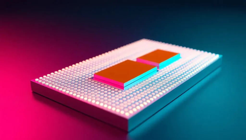
In recent years, the global semiconductor landscape has been characterized by rapid advancements and fierce competition. Among the key players vying for technological supremacy is Russia, which has unveiled an ambitious roadmap to develop its own Extreme Ultraviolet (EUV) lithography and X-ray technologies. This initiative aims to produce chips ranging from 65 to 10 nanometers between 2026 and 2037, positioning Russia as a potential contender in the semiconductor industry.
This plan, announced by Dimitrii Kuznetsov, signifies a critical step for Russia as it seeks to establish a reliable alternative to existing lithography technologies, particularly focusing on cost-effectiveness and efficiency. Given the current state of the semiconductor industry, such advancements could reshape the competitive dynamics, especially if they manage to overcome the technological gaps that exist today.
Russia's ambitious timeline for EUV lithography by 2037
The Institute of Microstructure Physics of the Russian Academy of Sciences has laid out a detailed roadmap that outlines milestones leading up to 2037. Starting in 2026, the first goal is to achieve a stepper for 40 nm nodes, featuring two-mirror optics and a precision alignment of 10 nm. This initial stage is critical as it sets the foundation for subsequent advancements.
According to Kuznetsov's statements shared on social media, the timeline for Russia indicates a deliberate push to shorten development periods. By 2029–2032, the expectation is to transition to a 28 nm scanner capable of reaching 14 nm. This equipment will incorporate four mirrors, a 26×0.5 mm exposure field, and productivity levels exceeding 50 W/h. While Western companies, particularly ASML, have achieved these benchmarks over a decade ago, Russia’s progress, albeit slower, demonstrates a commitment to catching up.
By the period of 2033–2036, the ambition extends to scanners capable of 13 nm and even 9 nm processes, utilizing six mirrors, achieving a 2 nm alignment precision, and delivering yields of over 100 W/h. Such advancements could potentially bring Russia closer to current industry standards, marking significant progress in their technological capabilities.
Unique technological approach: Moving away from ASML
Unlike ASML, which has dominated the EUV lithography market, Russia is opting for a different technological pathway. This approach promises to leverage hybrid solid-state lasers, xenon plasma sources instead of tin, and mirrors made of ruthenium and beryllium to operate at a wavelength of 11.2 nm. This specific wavelength is pivotal as it allows for simplification of lithographic processes and reduction of costs compared to traditional EUV technologies that operate at 13.5 nm.
- Reduced production costs for nodes from 14 to 65 nm.
- Lower energy consumption, estimated at a third of current methods.
- Elimination of contamination issues related to tin.
This new approach is touted as a viable alternative to immersion lithography at 193 nm, highlighting Russia's ambition to not only catch up but to potentially innovate within the semiconductor manufacturing space. Additionally, Russia asserts that a portion of ASML’s foundational technology at 13.5 nm was influenced by contributions from Russian scientists, reinforcing their argument for legitimacy in the competitive landscape.
However, skepticism remains regarding their ability to deliver on this timeline, especially given their current lag in EUV technology. The 2037 timeline is ambitious, and the industry will be watching closely to see if they can indeed meet their targets. As Kuznetsov notes, "with the Russians, never say never," hinting at their historical resilience and potential for unexpected breakthroughs, especially with possible collaboration from China.
The geopolitical context of semiconductor production
The race for semiconductor supremacy is not only a technological challenge but also a geopolitical one. Countries are increasingly aware that control over semiconductor manufacturing is crucial for national security, economic stability, and technological independence. Russia's push into EUV lithography must be viewed within this broader context of international competition and collaboration.
- **National Security**: Semiconductors are critical for defense systems.
- **Economic Independence**: Reducing reliance on foreign technology.
- **Technological Sovereignty**: Building an indigenous tech ecosystem.
As nations vie for dominance in this vital sector, partnerships and alliances will play a significant role. The potential collaboration with China could provide Russia with access to resources and technologies that might accelerate their development timeline. However, this also raises concerns for Western nations, which may perceive such alliances as a threat to their own technological hegemony.
Challenges ahead for Russia's semiconductor ambitions
Despite the ambitious plans outlined, several challenges lie ahead for Russia in its quest for EUV lithography capabilities. These include:
- Technological Gaps: Existing competitors like ASML and TSMC have established a significant lead.
- Funding and Investment: Substantial investment will be required to develop and implement these technologies.
- Skilled Workforce: Attracting and retaining talent in a highly specialized field.
- Geopolitical Tensions: Sanctions and international relations may hinder access to critical technologies.
Addressing these challenges will require not only technological innovation but also strategic planning and international collaboration. The road ahead is fraught with uncertainty, yet the potential rewards could be transformative for the Russian semiconductor industry.
In a world increasingly reliant on advanced technology, the outcomes of Russia's ambitious plans for EUV lithography will have significant implications not only for their economy but for the global semiconductor industry as a whole. As we navigate this evolving landscape, staying informed about these developments will be crucial.
For a deeper insight into the geopolitical ramifications of these advancements, you can watch this video:


Leave a Reply