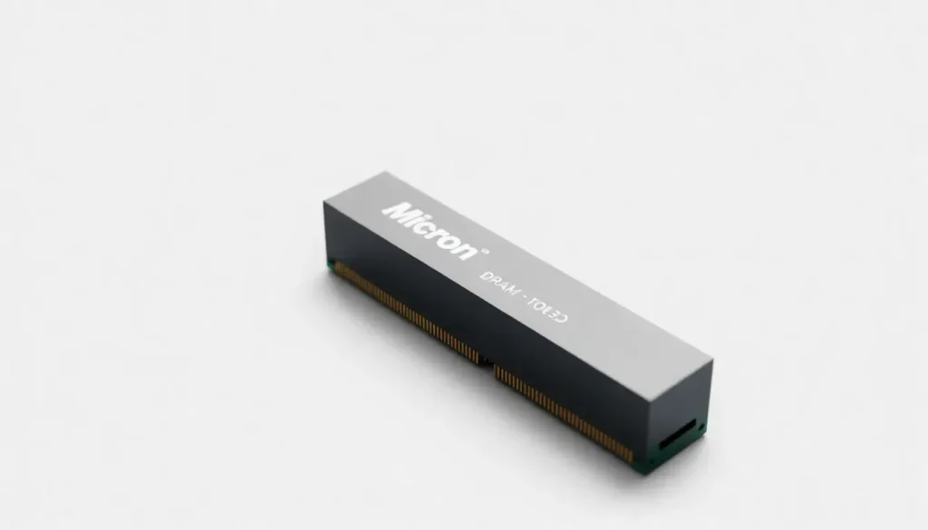
Micron Expands DRAM Roadmap to Infinitesimal Heights

In the rapidly evolving landscape of memory technology, Micron's latest updates to its DRAM roadmap signal significant advancements that could reshape the industry. With an aim to enhance efficiency and reduce production costs, the company is taking substantial steps towards smaller node sizes that promise greater capacity and performance. Let's delve into the details of this ambitious strategy.
Micron has recently revised its DRAM roadmap, introducing an additional stage in its cell shrink process, expanding from three to four distinct stages. This update is crucial as it aims to maximize DRAM capacity per wafer while simultaneously decreasing the cost per gigabyte, which is vital for manufacturers and consumers alike.
Understanding Micron's DRAM Process Node Strategy
The company plans to progressively decrease the size of its memory cells, transitioning from the now-obsolete 20nm process node size to a more compact 10nm (19nm-10nm range) node. This systematic reduction not only enhances the performance of the chips but also drives down manufacturing costs dramatically.
Micron's approach includes several critical nodes:
- 1Xnm – (c19-17nm) represents older DRAM technology.
- 1Ynm – (c16-14nm) is currently the mainstream DRAM bit production technology.
- 1Znm – (c13-11nm) accounted for 15% of Micron's DRAM bit production in Q3 2020.
- 1αnm – first volume production anticipated in the first half of 2021.
- 1βnm – currently in early development phases.
- 1ɣnm – involves early process integration.
- 1δnm – focused on pathfinding and may require EUV technology.
Among these, the 1δnm node introduces a new milestone in Micron's DRAM roadmap. However, specific process node sizes below 1Znm have yet to be disclosed, illustrating the company's ongoing innovation in this space.
Growth in Bit Density and Production Efficiency
While Micron has noted a slowdown in the growth rate of bit density during transitions from 1Xnm to 1Ynm and then to 1Znm, recent developments indicate a resurgence in efficiency. The company reported a remarkable 40% increase in growth rate transitioning to the 1αnm process node size, reflecting its commitment to optimizing production techniques.
In a recent analysis, Wells Fargo analyst Aaron Rakers emphasized Micron's dominant position in 1Znm DRAM output. According to research from DRAMeXchange, Micron's 1Znm production constituted 15% of its total DRAM bit production in Q3 2020, significantly outperforming competitors like Samsung and SK Hynix, which reported 6% and 0%, respectively.
Additionally, the cost-effectiveness of 1Znm DRAM is noteworthy. It is cheaper to manufacture compared to the previous 1Ynm node, which is a critical factor for Micron's competitiveness in the market.
Technological Innovations: The Role of EUV Lithography
Micron employs Deep Ultra Violet (DUV) multi-patterning lithography to define the DRAM cell die details on the wafer. However, as the size of the process nodes decreases below the 10nm threshold, the wavelength of the light used in lithography becomes a limiting factor.
To address this challenge, ASML, a leader in lithography machine manufacturing, has developed Extreme Ultra Violet (EUV) scanners. These machines utilize smaller wavelength light, enabling the etching of narrower lines on the wafer. This advancement facilitates smaller process sizes, allowing for more DRAM dies on each wafer, which in turn increases capacity and lowers costs per gigabyte.
Despite the advantages of EUV technology, there are significant financial considerations. Currently, ASML produces only 30 EUV lithography machines annually, each weighing an impressive 180 tons and costing around $120 million. This substantial capital requirement poses a barrier for many companies.
While Samsung has successfully integrated EUV technology into its 1Znm process nodes, and SK Hynix plans to adopt it for mass production of its 1αnm and 1βnm DRAM, Micron anticipates that EUV will not be cost-effective until 2023 or later, correlating with the development of the 1δnm process node.
Future Outlook: Micron's Competitive Edge
As Micron continues to innovate and adapt to market demands, its strategic roadmap positions the company favorably within the semiconductor industry. The shift to smaller node sizes and enhanced production efficiency is expected to drive demand for DRAM in various applications, from consumer electronics to enterprise-level solutions.
With the increasing reliance on data-intensive applications, the need for high-performance memory solutions will only grow. Micron's focus on delivering advanced DRAM technology aligns well with these trends, ensuring that it remains competitive in a rapidly changing market landscape.
For those interested in further exploring Micron's vision and innovations, check out the following video that outlines their roadmap for memory and storage technology:
In conclusion, Micron's proactive approach to enhancing its DRAM technology through innovative processes and efficient production techniques is a testament to its leadership in the semiconductor sector. As the demand for high-density memory continues to rise, Micron is poised to meet these challenges head-on.


Leave a Reply