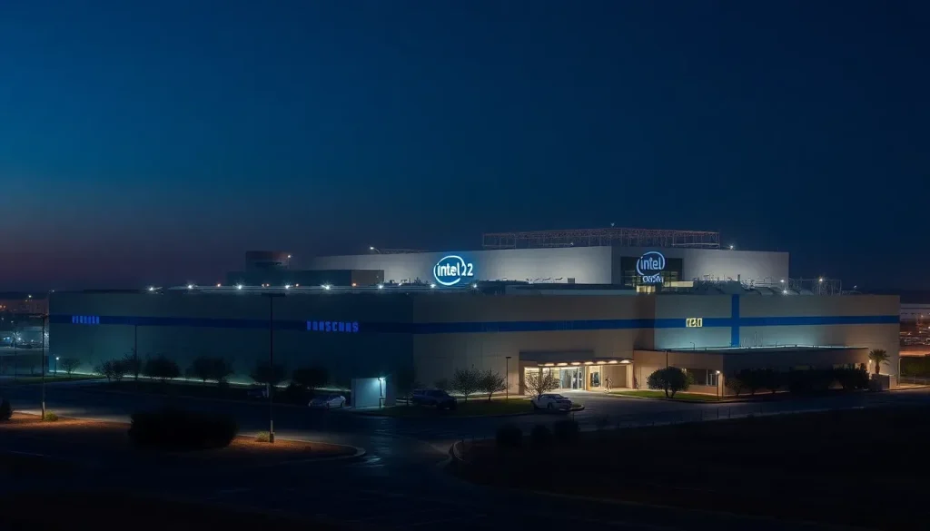
Intel Fab 52 in Chandler Arizona Operates 18A Technology
The semiconductor industry has been rapidly evolving, and Intel's recent developments in Chandler, Arizona, highlight the significant strides being made in this field. With the rise of semiconductor manufacturing in the U.S., particularly in Arizona, it's essential to understand the innovations and implications of Intel's latest technologies. This article delves into Intel Fab 52, its cutting-edge processes, and the broader context of semiconductor production in the region.
- Overview of Intel Fab 52 in Chandler
- Understanding the 18A Process Technology
- The Role of Advanced Equipment in Manufacturing
- Automation and Workforce in Semiconductor Manufacturing
- The Transformation of the Phoenix Area
- Environmental Considerations in Semiconductor Manufacturing
- Concluding Thoughts on the Future of Semiconductor Manufacturing in Arizona
Overview of Intel Fab 52 in Chandler
Located just a short drive from Phoenix, Intel Fab 52 stands as a testament to the company's long-standing commitment to semiconductor manufacturing in Arizona. The site has been operational for decades, and its significance has only grown as semiconductor demand skyrockets globally. Intel's Fab 52 is now at the forefront of producing next-generation chips using the innovative 18A process technology.
This facility, along with others in the region, positions Arizona as a critical hub in the semiconductor landscape. For instance, TSMC is also establishing advanced manufacturing facilities north of Phoenix, further cementing the area's reputation as a semiconductor powerhouse.
Understanding the 18A Process Technology
Intel's 18A process technology marks a pivotal advancement in the semiconductor manufacturing process. Among its most notable features are RibbonFET and PowerVia technologies, which promise to enhance performance and efficiency significantly.
- RibbonFET: This next-generation transistor technology enables improved electrical characteristics, allowing for better performance and efficiency in chip design.
- PowerVia: By repositioning power delivery to the backside of the chip, this innovation reduces interference and improves overall circuit performance.
- Cost Efficiency: Despite its advanced features, Intel has managed to keep the implementation costs low, enabling broader adoption of these technologies.
Intel claims that chips manufactured using the 18A technology can achieve over a 15% performance increase per watt compared to previous generations or reduce power consumption by 25% while maintaining the same performance levels. This advancement not only enhances Intel's product offerings but also positions the company favorably against competitors in the high-performance computing space.
The Role of Advanced Equipment in Manufacturing
A significant factor contributing to the success of Fab 52 is the advanced manufacturing equipment provided by companies like ASML. This equipment is pivotal in achieving the high yields needed for modern semiconductor production.
Although photos inside the fab are restricted, the sight of these sophisticated machines operating is a clear indicator of the technological prowess at play. The scale of the semiconductor manufacturing process is enormous, involving not just surface-level operations but also multi-level systems that enhance productivity.
Automation and Workforce in Semiconductor Manufacturing
The manufacturing process at Intel's fabs, including Fab 52, is highly automated. However, a skilled workforce remains essential for maintaining these intricate systems. Employees play a crucial role in ensuring that the machinery operates efficiently, akin to how a cobbler would maintain the tools necessary for shoemaking.
- Machine Maintenance: Workers focus on keeping the manufacturing tools in optimal condition.
- Robotics and Automation: Robots transport wafers through the facility, minimizing human contact and contamination.
- Specialized Roles: Employees have diverse roles that include engineering, quality control, and operational management.
This synergy between automation and human expertise allows for a seamless production environment that can adapt to the ever-evolving demands of the semiconductor market.
The Transformation of the Phoenix Area
The growth of semiconductor manufacturing in Arizona has significantly transformed the region. Once primarily agricultural land, Chandler has evolved into a thriving tech hub, hosting thousands of residents and numerous high-tech facilities.
Some key factors contributing to this transformation include:
- Strategic Location: Proximity to major markets like Los Angeles without the risk of natural disasters such as hurricanes or earthquakes.
- Infrastructure Development: Extensive investment in specialized infrastructure to support high-tech industries.
- Water Management: Efficient use of water resources, crucial for both semiconductor fabrication and agriculture.
The local economy has benefitted tremendously from this shift, with Intel's investment playing a pivotal role in attracting other businesses and fostering innovation.
Environmental Considerations in Semiconductor Manufacturing
As semiconductor manufacturing expands, so does the need for sustainable practices. Intel has made strides in this area, particularly concerning water usage. Arizona's water scarcity has led to a culture of conservation, influencing how fabs operate.
For instance, the recycling and treatment of wastewater generated by the manufacturing process are vital. This practice not only minimizes environmental impact but also ensures a sustainable water supply for future operations.
Concluding Thoughts on the Future of Semiconductor Manufacturing in Arizona
Visiting Intel Fab 52 was an eye-opening experience, showcasing the intricate processes behind modern chip manufacturing. With the ongoing innovations brought by the 18A technology and the expansion of facilities like Fab 52, Arizona is poised to become a leader in the global semiconductor market.
As the demand for high-performance chips continues to rise, the Phoenix area is set to play a crucial role in meeting these needs. The investments made by companies like Intel not only enhance technological capabilities but also contribute to the local economy, signaling a bright future for semiconductor manufacturing in the region.
For those interested in a visual representation of these advancements, you can watch this insightful video that provides an overview of the impressive facilities at Intel:


Leave a Reply